(Hong Kong)

Product Summary
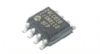
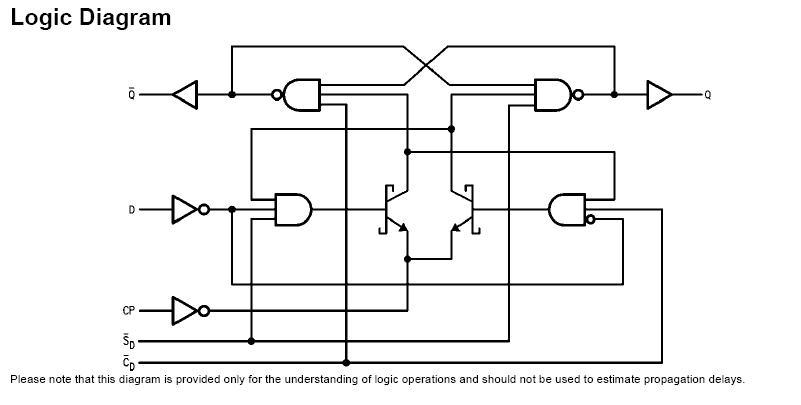
The 74F74SCX is a Dual D-Type Positive Edge-Triggered Flip-Flop with Direct Clear and Set inputs and complementary (Q, Q) outputs. Information at the input is transferred to the outputs on the positive edge of the clock pulse. Clock triggering occurs of the 74F74SCX at a voltage level of the clock pulse and is not directly related to the transition time of the positive-going pulse. After the Clock Pulse input threshold voltage has been passed, the Data input is locked out and information present will not be transferred to the outputs until the next rising edge of the Clock Pulse input.
Parametrics
74F74SCX absolute maximum ratings: (1)Storage Temperature: -65℃ to +150℃; (2)Ambient Temperature under Bias: -55℃ to +125℃; (3)Junction Temperature under Bias: -55℃ to +150℃; (4)VCC Pin Potential to Ground Pin: -0.5V to +7.0V; (5)Input Voltage (Note 2): -0.5V to +7.0V; (6)Input Current (Note 2): -30mA to +5.0mA; (7)Voltage Applied to Output in HIGH State (with VCC = 0V); (8)Standard Output: -0.5V to VCC; (9)3-STATE Output: -0.5V to +5.5V; (10)Current Applied to Output in LOW State (Max): twice the rated IOL (mA); (11)ESD Last Passing Voltage (Min): 4000V.
Features
74F74SCX features: (1)VIH Input HIGH Voltage: 2.0V Min; (2)VIL Input LOW Voltage: 0.8V Max; (3)VCD Input Clamp Diode Voltage: -1.2V Max; (4)VOH Output HIGH Voltage 10% VCC: 2.5V Min; (5)5% VCC: 2.7V Min; (6)Output LOW voltage 10% VCC: 0.5V Max; (7)Input HIGH Current: 5.0μA Max.
Diagrams
| Image | Part No | Mfg | Description |  |
Pricing (USD) |
Quantity | ||||
|---|---|---|---|---|---|---|---|---|---|---|
 |
 74F74SCX |
Fairchild Semiconductor |
Flip Flops Dl D-Type Flip-Flop |
Data Sheet |
Negotiable |
|
||||
 |
74F74SCX_NL |
Fairchild Semiconductor |
Flip Flops FINISHED GOOD |
Data Sheet |
Negotiable |
|
||||