(Hong Kong)

Product Summary
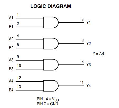
The 74HC08PW is a Quad 2-Input AND Gate. The 74HC08PW is identical in pinout to the LS08. The 74HC08PW inputs are compatible with Standard CMOS outputs; with pullup resistors, they are compatible with LSTTL outputs.
Parametrics
74HC08PW absolute maximum ratings: (1)VCC, DC Supply Voltage (Referenced to GND): – 0.5 to + 7.0 V; (2)Vin, DC Input Voltage (Referenced to GND): – 0.5 to VCC + 0.5 V; (3)Vout, DC Output Voltage (Referenced to GND): – 0.5 to VCC + 0.5 V; (4)Iin, DC Input Current, per Pin: ±20 mA; (5)Iout, DC Output Current, per Pin :±25 mA; (6)ICC, DC Supply Current, VCC and GND Pins: ±50 mA; (7)PD, Power Dissipation in Still Air: 500 mW; (8)Tstg, Storage Temperature: – 65 to + 150℃; (9)TL, Lead Temperature: 260℃.
Features
74HC08PW features: (1)Output Drive Capability: 10 LSTTL Loads; (2)Outputs Directly Interface to CMOS, NMOS and TTL; (3)Operating Voltage Range: 2.0 to 6.0 V; (4)Low Input Current: 1.0 μA; (5)High Noise Immunity Characteristic of CMOS Devices; (6)In Compliance With the JEDEC Standard No. 7A Requirements; (7)ESD Performance: HBM 2000 V; Machine Model > 200 V; (8)Chip Complexity: 24 FETs or 6 Equivalent Gates; (9)These are Pb-Free Devices.
Diagrams
| Image | Part No | Mfg | Description |  |
Pricing (USD) |
Quantity | ||||||||||||
|---|---|---|---|---|---|---|---|---|---|---|---|---|---|---|---|---|---|---|
 |
 74HC08PW,112 |
NXP Semiconductors |
Gates (AND / NAND / OR / NOR) QUAD 2-INPUT AND |
Data Sheet |
|
|
||||||||||||
|
74HC08PW,118 |
NXP Semiconductors |
Gates (AND / NAND / OR / NOR) QUAD 2-INPUT AND |
Data Sheet |
|
|
||||||||||||