(Hong Kong)

Product Summary
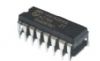
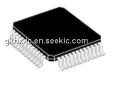
The CDCLVP110VF is a clock driver. It distributes one differential clock pair of either LVPECL or HSTL (selectable) input, (CLK0, CLK1) to ten pairs of differential LVPECL clock (Q0, Q9) outputs with minimum skew for clock distribution. The CDCLVP110VF can accept two clock sources into an input multiplexer. The CLK0 input accepts either LVECL/LVPECL input signals, while CLK1 accepts an HSTL input signal when operated under LVPECL conditions. The CDCLVP110VF is specifically designed for driving 50-Ω transmission lines.
Parametrics
CDCLVP110VF absolute maximum ratings: (1)VCC Supply voltage: –0.3 to 4.6 V; (2)VI Input voltage: –0.3 to VCC + 0.5 V; (3)VO Output voltage: –0.3 to VCC + 0.5 V; (4)IIN Input current: ±20 mA; (5)VEE Negative supply voltage: –0.3 to 4.6 V; (6)IBB Sink/source current: –1 to 1mA; (7)IO DC output current: –50mA; (8)Tstg Storage temperature range: –65 to 150℃.
Features
CDCLVP110VF absolute maximum ratings: (1)VCC Supply voltage: –0.3 to 4.6 V; (2)VI Input voltage: –0.3 to VCC + 0.5 V; (3)VO Output voltage: –0.3 to VCC + 0.5 V; (4)IIN Input current: ±20mA; (5)VEE Negative supply voltage: –0.3 to 4.6 V; (6)IBB Sink/source current: –1 to 1mA; (7)IO DC output current: –50mA; (8)Tstg Storage temperature range: –65 to 150℃.
Diagrams

| Image | Part No | Mfg | Description |  |
Pricing (USD) |
Quantity | ||||||||||||
|---|---|---|---|---|---|---|---|---|---|---|---|---|---|---|---|---|---|---|
 |
 CDCLVP110VF |
Texas Instruments |
Clock Drivers & Distribution 1:10 CLOCK DRIVER |
Data Sheet |
|
|
||||||||||||
|
CDCLVP110VFG4 |
Texas Instruments |
Clock Drivers & Distribution 1:10 CLOCK DRIVER |
Data Sheet |
|
|
||||||||||||
|
CDCLVP110VFRG4 |
Texas Instruments |
Clock Drivers & Distribution 1:10 CLOCK DRIVER |
Data Sheet |
|
|
||||||||||||
|
CDCLVP110VFR |
Texas Instruments |
Clock Drivers & Distribution 1:10 CLOCK DRIVER |
Data Sheet |
|
|
||||||||||||