(Hong Kong)

Product Summary
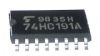
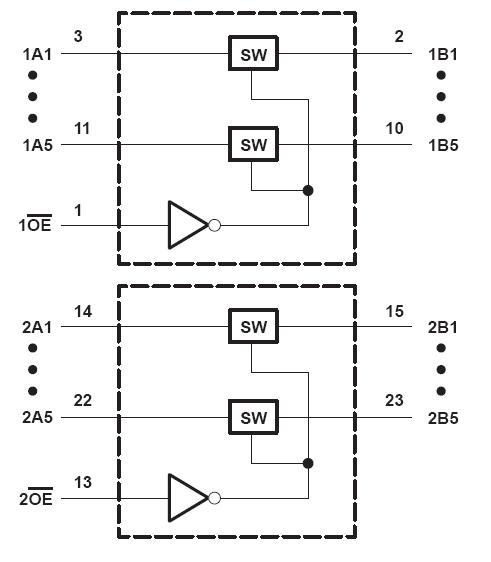
The SN74CBTD3384CDWR is a high-speed TTL-compatible FET bus switch with low ON-state resistance (ron), allowing for minimal propagation delay. The SN74CBTD3384CDWR features an integrated diode in series with VCC to provide level shifting for 5-V input down to 3.3-V output levels. Active Undershoot-Protection Circuitry on the A and B ports of the SN74CBTD3384CDWR provides protection for undershoot up to -2 V by sensing an undershoot event and ensuring that the switch remains in the proper OFF state.
Parametrics
SN74CBTD3384CDWR absolute maximum ratings: (1)Supply voltage range, VCC: -0.5 V to 7 V; (2)Control input voltage range, VIN (see Notes 1 and 2): -0.5 V to 7 V; (3)Switch I/O voltage range, VI/O (see Notes 1, 2, and 3): -0.5 V to 7 V; (4)Control input clamp current, IIK (VIN<0): -50mA; (5)I/O port clamp current, II/OK (VI/O<0): -50mA; (6)ON-state switch current, II/O (see Note 4): ±128mA; (7)Continuous current through VCC or GND terminals: ±100mA; (8)Package thermal impedance, θJA (see Note 5): DB package: 63℃/W; (9)DBQ package: 61℃/W; (10)DGV package: 86℃/W; (11)DW package: 46℃/W; (12)PW package: 88℃/W; (13)Storage temperature range, Tstg: -65℃ to 150℃.
Features
SN74CBTD3384CDWR features: (1)Undershoot Protection for Off-Isolation on A and B Ports Up To -2V; (2)Integrated Diode to VCC Provides 5-V Input Down To 3.3-V Output Level Shift; (3)Bidirectional Data Flow, With Near-Zero Propagation Delay; (4)Low ON-State Resistance (ron) Characteristics (ron = 3 Ω Typical); (5)Low Input/Output Capacitance Minimizes Loading and Signal Distortion (Cio(OFF) = 5 pF Typical); (6)Data and Control Inputs Provide Undershoot Clamp Diodes; (7)VCC Operating Range From 4.5 V to 5.5 V; (8)Data I/Os Support 0 to 5-V Signaling Levels (0.8-V, 1.2-V, 1.5-V, 1.8-V, 2.5-V, 3.3-V, 5-V); (9)Control Inputs Can be Driven by TTL or 5-V/3.3-V CMOS Outputs; (10)Ioff Supports Partial-Power-Down Mode Operation; (11)Latch-Up Performance Exceeds 100 mA Per JESD 78, Class II; (12)ESD Performance Tested Per JESD 22: 2000-V Human-Body Model (A114-B, Class II); (13)1000-V Charged-Device Model (C101); (14)Supports Both Digital and Analog Applications: Memory Interleaving, Bus; (15)Isolation, Low-Distortion Signal Gating.
Diagrams
| Image | Part No | Mfg | Description |  |
Pricing (USD) |
Quantity | ||||||||||||
|---|---|---|---|---|---|---|---|---|---|---|---|---|---|---|---|---|---|---|
 |
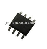
 SN74CBTD3384CDWR |
Texas Instruments |
Digital Bus Switch ICs 10-Bit FET Bus Switch |
Data Sheet |
|
|
||||||||||||
|
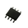
SN74CBTD3384CDWRE4 |
Texas Instruments |
Digital Bus Switch ICs DUAL INVERTER |
Data Sheet |
|
|
||||||||||||
|
SN74CBTD3384CDWRG4 |
Texas Instruments |
Digital Bus Switch ICs 10B FETBus Switches |
Data Sheet |
|
|
||||||||||||